USB Endpoint 0
As discussed before, USB Endpoint 0 is used for all "control" transfers. That is to say that all setup and all requests for device information (not data like keystrokes or mouse movements etc) will be done using endpoint 0. It is thus a special endpoint and as such it has its own set of registers on the PIC32MZ.
In all the time I spent trying to get USB host mode to work, the thing that was holding me back was my understanding of a single register named USBE0CSR0 (for some reason called USBIE0CSR0 in the datasheet). Never mind that they changed the name in the code and not in the datasheets, let's look at this register:
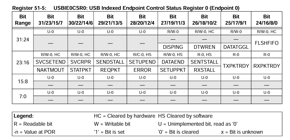
The first thing you'll notice is that the lower two bytes are unused, as well as the upper four bits. So what is this register used for? To put it simply, it is used to perform all the handshakes you need in the enumeration of the USB device you are wanting to connect to. If you do not understand this register, you will be doomed to two years of on-again-off-again futile effort, trying desperately to read Harmony code. If only Microchip ever explained what these bitfields mean and how they use them, hey? I guess they're too busy writing Harmony 4, which will undoubtedly be incompatible with Harmony 3 code and also require you to include freeRTOS to get anything done. Yay.
Sending a setup packet
But I digress. Here is how you send a setup packet via USB Endpoint 0:
To send a setup packet, you load the data into USBFIFO0 as usual. You then must set the TXPKTRDY and the SETUPPKT bits. I do it like this (as does Harmony):
*((unsigned char*)&USBE0CSR0 + 0x2) = 0xA;
OK, we have now sent the packet. For example, if we want to do a GET DEVICE DESCRIPTOR request, we would load
0x80 0x06 0x00 0x01 0x00 0x00 0x12 0x00
into USBFIFO0 and then set
*((unsigned char*)&USBE0CSR0 + 0x2) = 0xA;
That part is easy enough to understand. Once the device gets the request, it will trigger an interrupt on the PIC32MZ, and set the EP0IF flag in the USBCSR0 register.
Please remember that if you read the USBCSR0, USBCSR1, USBCSR2 or USBCSR3 registers EVEN ONCE they are cleared! Always do something like the following:
unsigned int CSR0;
unsigned char EP0IF;
CSR0 = USBCSR0;
EP0IF = (CSR0 & (1<<16)) ? 1 : 0;
Once an interrupt has been triggered, we move on to the next step, which is getting the data we requested in GET DEVICE DESCRIPTOR.
Reading data from a connected device
Sending the "ready to receive" handshake
OK, so we sent the setup packet and the device gave us a handshake. Does the data now appear on USB Endpoint 0? No. USB is a series of handshakes. We now need to tell the device OK, we're ready to receive the packet. We do this by setting the REQPKT flag in USBE0CSR0, like this:
*((unsigned char*)&USBE0CSR0 + 0x2) = 0x20; // REQPKT
Now that we've sent the magic "hey, I'm ready to receive" handshake, we wait again for the device to send an interrupt signalling it's ready to receive.
Reading the data sent from the device
When this happens, you will find the number of bytes sent in USBE0CSR2bits.RXCNT; and the data will be available in USBFIFO0, which you must read out to clear the buffer. You then need to set USBE0CSR0bits.RXRDYC = 1;. Why am I setting the bitfield directly there and not in the fancy way I did before? Well, to be honest this code is like a magic spell to me. This is how Harmony does it and it works, so I'm using it :)
The device will not trigger an interrupt after you set RXRDYC = 1;
Sending the "OK I've received the data, thanks dude" handshake
After you've received the data, you must then send the device a handshake telling it you received it. But look at that USBE0CSR0 register again. How would you do that? Well, dear reader, it turns out the answer is to set the TXPKTRDY bit field! At this point, you also need to set the STATPKT bitfield. This, to quote the datasheet, "1 = When set at the same time as the TXPKTRDY or REQPKT bit is set, performs a status stage transaction."
Harmony, and I, do it like this:
*((unsigned char*)&USBE0CSR0 + 0x2) = 0x42; // STATUS + TXPKTRDY
OK, what is a "status transition"?
OK I'll be honest with you guys. I'm not 100% sure. But what I think it means is "we're doing with this transaction now". And I can tell you with certainty that if you don't set STATPKT and TXPKTRDY at the end here, your device will stop responding :)
My device sent me 64 bytes, I did as you said and now it's stopped responding. You are a liar, a thief and a traitor!
Hang on, hang on. OK there is one more thing to add. If you know anything about USB devices you will know that they have a limit in how much they can send at once. For low speed devices, this is typically 8 bytes. For full speed devices like my keyboard, this is typically 64 bytes. This means that if a full speed device needs to send you 65 bytes, it will have to send you two packets. So the reading works like this:
- Send setup packet as normal
- Set
TXPKTRDY and SETUPKT as normal
- Wait for interrupt
- Set
REQPKT by setting *((unsigned char*)&USBE0CSR0 + 0x2) = 0x20;
- Wait for the handshake
- Read from
USBFIFO0
- Send the "received" handshake by setting
USBE0CSR0bits.RXRDYC = 1;
- Still wanting more data? Go back to step 3 and repeat as many times as necessary.
- When done, remember to set
STATPKT and TXPKTRDY to let the device know that you're done!
- Wait for the device to acknowledge and thus trigger an interrupt before moving on
Sending a command, but not wanting any data back
There are commands that don't require us to read any data back at all. For example, the SET IDLE command. How do we handle those? They're very similar with a slightly different handshake:
- Send setup packet as normal
- Wait for an interrupt
- Set
STATKT and REQPKT, by setting *((unsigned char*)&USBE0CSR0 + 0x2) = 0x60;
- Wait for an interrupt
- Clear
STATPKT and REQPKT, by setting *((unsigned char*)&USBE0CSR0 + 0x2) &= 0x41;
- No interrupt will be generated now, you are free to move on
As you can see, as opposed to when we're reading a packet we immediately request a status transition by setting STATPKT. The trick for me was that you also have to set REQPKT or TXPKTRDY in order for this to cause a handshake to be sent. In this case, although we are not going to receive any data, we need to set REQPKT to get the handshake to go out.
Sending a command AND data to the device
OK, this sounds simple right? No, sadly not. This one tricked me.
The command I wanted to use was the SET REPORT command, which I was wanting to use to tell the keyboard to turn on or off LEDs. It's simply the SET REPORT command, which looks like this:
0x21 0x09 0x00 0x02 0x00 0x00 0x01 0x00
and then followed by a single byte of data. I thought, foolishly, that you could just send 9 bytes of data to the device and it'd work. But no, it doesn't quite work like that. Here are the actual steps involved:
- Send setup packet as normal (i.e. set
SETUPPKT and TXPKTRDY)
- Wait for an interrupt
- Immediately send out the data on EP0, but do not set
SETUPPKT, only set TXPKTRDY
- Wait for an interrupt
- Set
STATPKT and REQPKT, by setting *((unsigned char*)&USBE0CSR0 + 0x2) = 0x60;
- Wait for an interrupt
- Clear
STATPKT and REQPKT, by setting *((unsigned char*)&USBE0CSR0 + 0x2) &= 0x41;
- No interrupt will be generated now, you are free to move on
It is very, very important to remember that if setup packets contain data, that data is not part of the initial command. It is sent separately immediately after the device acknowledges it has received the command and it is not sent as a setup packet.
I know all this stuff sounds super obvious now, but believe me it took me many painful hours to come to grips with it all.
OK phew, that's a lot to digest. Perhaps no one will ever read this, but I think this information needs to be out there.
Next time I'll go over what's actually involved in enumerating and getting a device to work on your PIC32MZ board in USB host mode, because some stuff like SET ADDRESS doesn't work as you'd expect. Of course! :)