My PIC32MZ Dev Board post
Disclaimer
The files / images I'm sharing today are for my own personal development board, based on the PIC32MZ2048EFH144-I/PL. Do not use this board in any project that requires super precision or in life saving equipment type of projects. I cannot and will not be responsible if you make this and somehow manage to burn your house / neighbourhood / country down. I'm uploading them in the hopes that someone starting out can learn how to make their own PIC32MZ development board, hopefully better than my own.
Background on why I started making my own dev boards
When I first started with the PIC32, the dev board options weren't awesome. I was looking using the PIC32MX in a DIP package, so it could be bread-boarded. I found myself wanting a more permanent solution and decided to look into what development boards there were available. Microchip and other companies' dev boards are fine and all, some of them aren't even too expensive. However, they're often either designed with a very specific purpose in mind or designed to attach to other dev boards of theirs and the cost very quickly gets out of control. I just wanted something I could plug Dupont cables into and I couldn't find what I was looking for, so I decided to make my own.
I pretty soon got into making my own PCBs at home using a laser printer, iron-on paper, an iron and some etchant. For years I made my own boards and they were fine. When it came to the PIC32MZ I was able to make my own PCB for the 144-pin version but I quickly began to realise the limitiations of making single-sided PCBs. You can make double-sided PCBs at home but you have to be very careful to line up both sides correctly, drill the vias, solder the via pins in, etc and it turns into a lot of work very quickly. I also got tired of breathing in fiber glass when drilling all the holes for the headers. It may not seem like a lot but 200 holes done repeatedly gets a bit much. The etchant had already eaten holes in a good few pairs of pants too and I finally decided enough was enough and started looking online.
I first used Seeedstudio's excellent Fusion PCB service and found the quality to be great. I also appreciate that the different PCB colours don't cost any extra money. An alternative to them is JLCPCB. Their service is slightly cheaper and has faster and more reliable turn-around times but you have to pay extra for any PCB colour except green. A huge advantage with JLCPCB is that you can order components at their sister site LCSC and use combined shipping to save on those painful DHL shipping costs, which for me come to about $16.
Down-sides of making your own dev board
First of all, all the Harmony examples are set up to use their own dev boards, so whenever I want to use an example I have to modify code for LEDs and buttons. That's not too much bother really. The big problem, however, is that
BOARDS DESIGNED BY NOOBS LIKE ME BREAK TONS OF DESIGN RULES
While Seeedstudio and JLCPCB's prices are both good, you can get really cheap prices if you fit the board into 100mm x 100mm, double-layer. So my dev boards represent an effort to cram as much stuff as I can into that size limit while still having a working board. As such, there are too many vias, fast signals tracks are too long and routed through vias as they shouldn't be and the power and ground planes are probably more of a mess than they need be, despite multiple efforts to clean them up. Now, that out the way, my boards work fine. The USB is as fast as it should be, the ESP32 works, the SD card can be read at a very decent speed, everything works. If you can get over the worry of having an engineer looking at your board in disgust, then you too can make your own PIC32MZ dev board.
So why? Well, this is my hobby, I enjoy it. I use my dev boards to get modules, motors, LCDs and all sorts of things to work before designing specific boards for separate projects. It's a kitchen sink. A very clogged up kitchen sink. And today I'm going to share all the files for it with the Internet. If anyone even reads this, I'm sure they'll leave some delightful comments but eh, I'm uploading them all the same.
Overview of this dev board
First, this is what it looks like when assembled by a noob (me). Top:
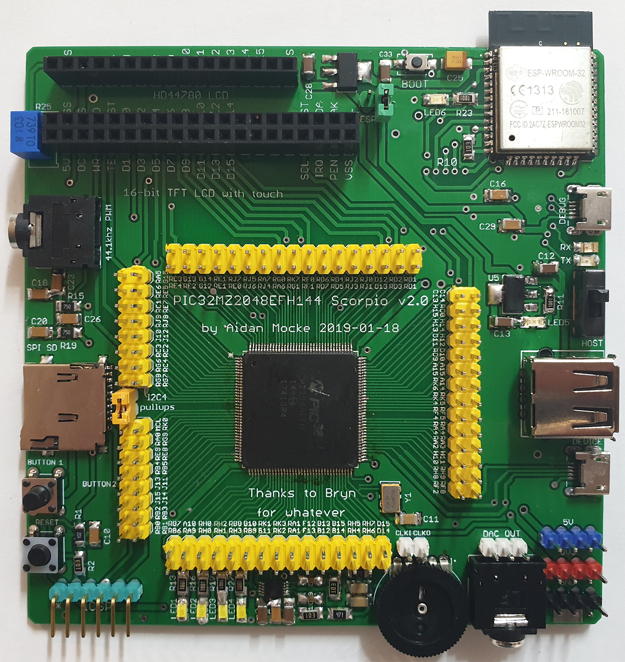
Yes, the erroneous "BUTTON 2" text has been removed in the uploaded Gerber files.
Bottom:
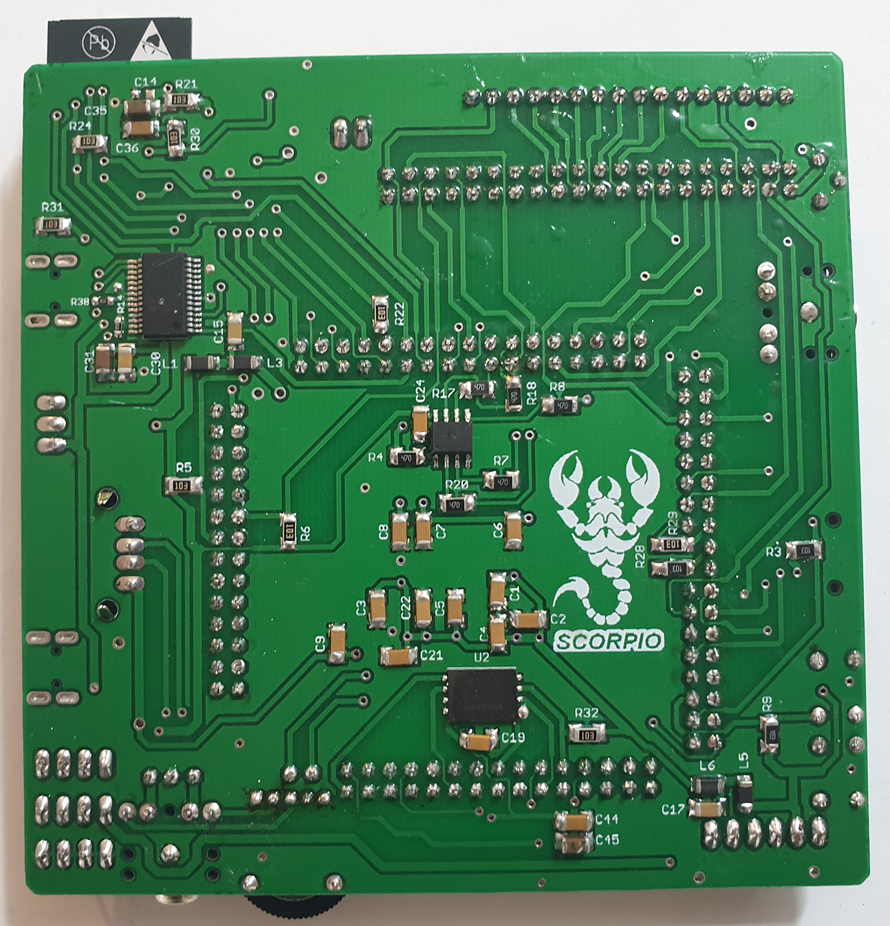
Yes, the scorpion motif was cheesy as heck and has been removed (also, it was downloaded from a royalty free clipart site I can no longer find the link for).
This dev board, being based on a kitchen sink design philosophy, has a lot going on with it. Most of the extras can be left out entirely without affecting the PIC32 at all. I will mark these extras with a *. The list:
- SD card attached in SPI mode to SPI channel 2 (*)
- CS4344 audio DAC attached in I2S mode to SPI3 (*)
- 8MB VTI7064 PSRAM attached via SQI (*)
- 128MB W25N01GV flash memory attached to SPI5 (*)
- Parallel Master Port (PMP) driver 16-bit TFT LCD connector for SSD1934 displays with capacitive touch (*)
- HD44780 compatible text LCD port connected to the PMP (*)
- FT232RL connected to UART4 to allow communications with PC (*)
- USB host connector (*)
- Stereo PWM audio output connector with single stage RC filter designed to work at 44.1kHz (*)
- ESP32-WROOM-32 module connected to UART2 and SPI1, with connections to allow PIC32 and ESP32 to wake each other (*)
- Power via micro USB port in either debug mode (with FT232RL) or device mode (two separate ports)
So basically, a lot of stuff, some of which is a hassle to solder by hand and none of which is necessary except for the USB port which provides power to the PIC32 chip. If you don't even want that, you could also power it directly via the ICSP connector using a PICKit or other programmer but bear in mind that needs to be 3.3V.
The ESP32 has been added very recently and in rather a slap-dash fashion. It is supplied by it's own 3.3V regulator and can be entirely disabled by removing the jumper near it labelled "ESP32".
I have tried to use 1206 sized SMD components to make it easier to hand solder but there are one or two places where I ran out of space (/willpower) and so used 0603.
Bill of Materials (BOM) and where to buy the components
I have put together a list of components for use when soldering and a Bill of Materials with links showing where to buy the components.
Here are the Gerber files for this project.
Here are the Eagle files for this project.
Almost, but not all, of my example code on this site was made with these ports in mind.
Categories: pic32